- Apr 17, 2011
- 9,228
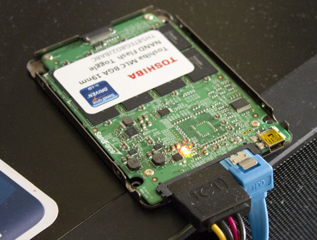
Toshiba’s 19nm NAND flash technology has been demonstrated in SSD products using SandForce’s 2281 controller at this year’s Computex.

These new memory chips should bring the SSD prices further down and, hopefully, will also maintain the NAND durability that has decreased dramatically since the times of the 35nm technology.
The durability of flash cells inside today’s solid state drives is quite an important issue of the technology.
The main concern is the ability of the drive to undergo repeated writes and erases of the same NAND cell. Every subsequent write and erase of a single NAND flash cell is called a P/E cycle.
Writing to a cell is usually expressed as “programming” a cell. Hence the expression program/erase cycle (P/E).
In the 35nm times, SSD drives were certified for over 30,000 P/E cycles. Burning through the usability of a SSD was virtually unachievable.
Unfortunately today, SSD drives are usually certified for only 3000 P/E cycle with a bunch of “higher grade” products that are rated for 5000 P/E cycles.
Honestly we wouldn’t know how the end-user could check and monitor this on his home unit in an easy and handy manner.
There is much anxiety about decreased P/E cycle ratings on SSDs that use newer and smaller NAND.
Intel and Micron are moving their manufacturing facilities to 20nm technology while Toshiba has a small edge on them using 19nm flash.
The first move expected is a 10% decrease in price per gigabyte in SSDs using the newer technologies and performance ratings are just the same at 500 MB/s.
TechReport has reportedly managed to see some early test drives using Toshiba’s TOGLE 19nm flash and Intel and Micron’s new chips paired up with LSI’s SandForce controllers.
The tests showed a performance around 500 MB/s in 128KB sequential reads and writes and 60,000 IO operations in 4KB random writes.
Source

