At the
IEDM conference, TSMC charted a course to delivering chip packages with one trillion transistors, much like
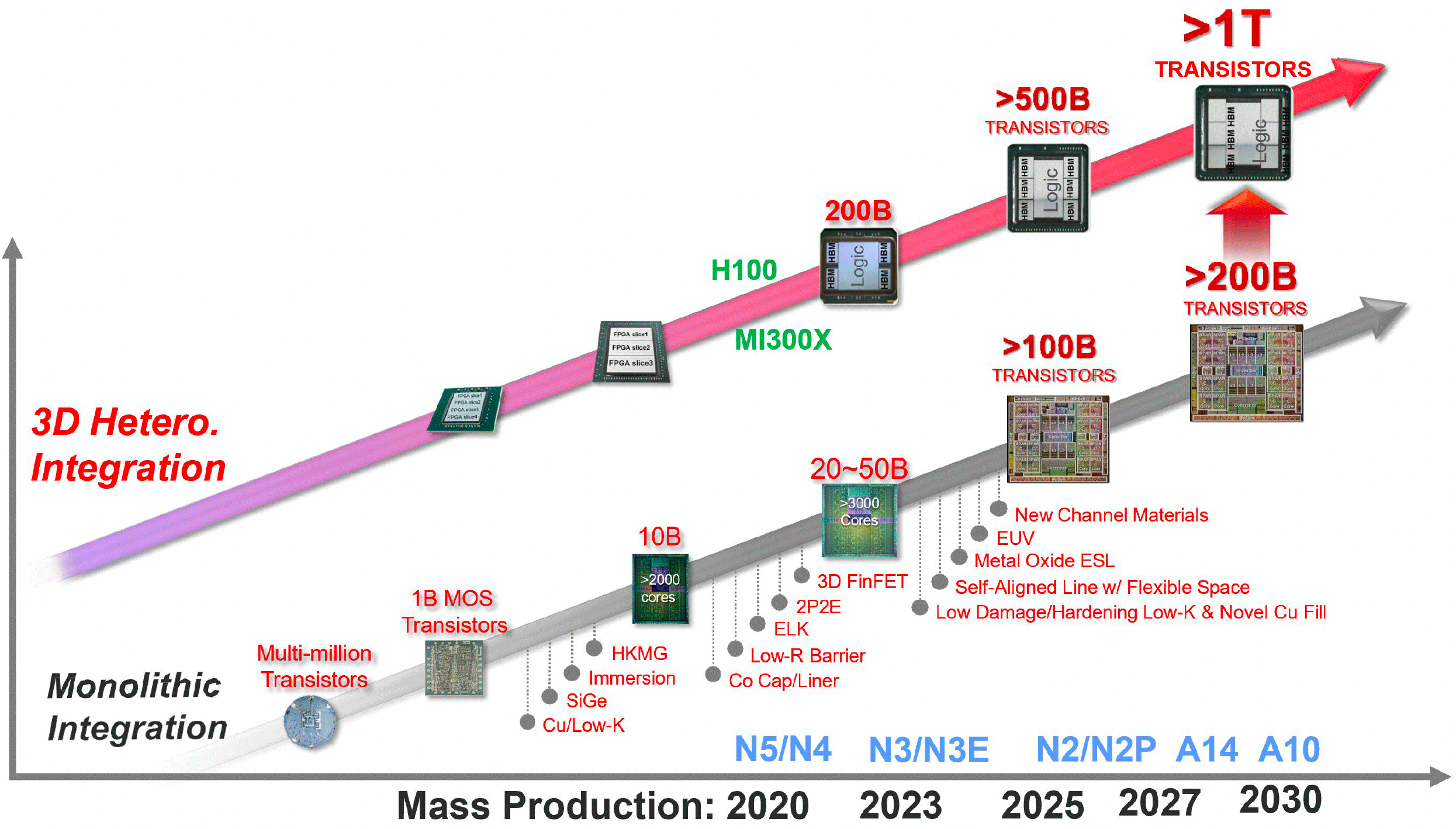
Intel divulged last year. Those behemoths will come courtesy of 3D-packaged collections of chiplets on a single chip package, but TSMC is also working to develop chips with 200 billion transistors on a single piece of silicon. To meet that goal, the company reaffirmed that it is working on 2nm-class N2 and N2P production nodes and 1.4nm-class A14 and 1nm-class A10 fabrication processes that are due by 2030.
In addition, TSMC foresees advancements in packaging technologies (CoWoS, InFO, SoIC, etc.), allowing it to build massive multi-chiplet solutions packing more than a trillion transistors around 2030.
TSMC slide from IEDM conference foresees advancements in packaging technologies. (Image credit: TSMC)

